I have recently decided that enough was enough. I could not possibly go on without a 64K machine, so I upgraded my 400 (my only A8) to 64K. For those of you who wish to recreate what I did, this post is for you. Please read through this completely before you try it to get an idea of what it takes to do.
*****DISCLAIMER*****
I am not responsible for anything that happens because of this post. Good or bad. I don't care. I didn't do it. You use these directions at your own risk
Material Requirements
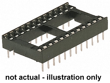
In no particular order:![Posted Image]() (socket in image is 24 pin, but shows the type you need. image taken from: http://www.soemtron....sktfacewipe.jpg)
(socket in image is 24 pin, but shows the type you need. image taken from: http://www.soemtron....sktfacewipe.jpg)
Open your atari 400 being carful not to pull on the keyboard ribbon cable while doing so. For more detailed instructions (recommended if you are not familiar with the process) consult the Atari 400/800 Field Service Manual. (pg. 74, Atari 400/800 Field Service Manual)
Step 2: Installing the 48K Card
Install the 48K ram upgrade as per the instructions provided by Atari if you have not already. Verify that it works using the tests described in the installation manual.
Step 3: Building the Atari 400 64K Conversion Circuit Board
Build the circuit shown in the schematic diagram shown below: (click for bigger image)
![Posted Image]()
Anywhere there is an input shown (like /S6) or an output (like /RAMEN) there will be a wire going from the circuit to somewhere else. NOTE: the switch is only shown for reference, do not mount the switch on your circuit, this switch needs to be mounted somewhere you can reach it. For now, leave the switch out completely. Also, do not forget about power pins. On the 7400 and 7402, the power pins are 14 (positive) and 7 (ground). You should install the .1uF capacitors across these pins (one on each chip) as well as connect the power pins of both chips together. This circuit board will be referred to as the 'Atari 400 64K conversion circuit board' from this point on.
Step 4: Modifying the 48K card
Remove the 48K ram board from the Atari 400 motherboard. It is time to make modifications to the 48K board. Start by completely removing R13. Next, remove U14 from it's socket and bend pins 3 and 6 outward so that they do not go back into the socket. Reinsert U14 and check proper orientation in the socket. Pins 3 and 6 should not be inside the socket.
Step 5: Attach the Atari 400 64K Conversion Circuit Board
In this step, you will begin wiring things together. Start by placing your Atari 400 64K conversion circuit board in the approximate position shown in the picture below. (the white thing with black electrical tape on it is the circuit board.)
![Posted Image]()
Refer back to the schematic diagram from step 3. Connect the following connections from the schematic to the points indicated on the 48K board:
Atari 400 64K conversion circuit - Atari 48K RAM board
/RAMEN - bottom of empty R13 spot
A12 - U10 pin 14
A13 - U10 pin 2
A11 - U9 pin 14
In addition to these, connect the positive supplies of the two IC's to the top of the empty R13 spot. Connect the GND pins of the two IC's to the top side of C4 (or any other place a ground connection can be obtained). you will notice there are two wires not mentioned. the A14 and A15 lines. These two connections need to be able to reach to the left side of the motherboard, fold under, reach all the way to the underside of Z103 (pins 13 & 14 specifically) and still have a little slack. I had a jagged edge to the left of the ram slot on my 400 motherboard that left room for the wires to run between the motherboard and the RF shield. If you don't have this, you will have to figure it out yourself. Sorry.
This is a good time for a little tip. Unless you are trying to conserve wire, it is alright to use too much wire. you can always cut wire off. What is more difficult (and looks bad) is when you need to add more wire. So don't make the mistake I did several times, and use lots of wire if you are unsure.
Step 6: Wiring the Rest of the Atari 400 64K Conversion Circuit Board Wires
Start by bending the angle between your Atari 400 64K conversion circuit board and your Atari 48K board to be about 90 degrees. Insert the 48K board into the Atari 400 motherboard. In this step, you need to measure out the amount of wire you need to make each connection.
If you refer back to the schematic, you will see that we have 4 connections left: /S6, /S7, /ROMEN, and the line going from the DPDT to pins 5, 6, and 9 of the 7402. /S6 and /S7 connect to two more pins on Z103, so make sure the wires you connect will reach back. /S6 connects to pin 7 of Z103 and /S7 connects to pin 9 of Z103. /ROMEN will go to the general area of the OSROM's, A103, A104, and A105, but leave no wire connected here for now. The DPDT wire should be about long enough to extend an inch or two outside of where the front of the 400 normally is. After you are done wiring these wires, the back of your motherboard around the Z103 area should look like this (except hopefully you didn't use wire with PVC insulation that melted):
![Posted Image]()
Step 7: Burn the EPROM
Grab the attached .bin file and burn it to your EPROM. Don't forget to put something opaque over the window in the EPROM after it has been programmed.
Step 8: Build a 27C256 --> Atari OSROM adapter
Now this bit I am not sure whether to be proud of or ashamed of. I unfortunately don't have pictures for this one, so you will have to use your imagination. Take the first 28 pin double wipe socket and bend pins 1, 2, 20, 22, 23, 26, 27, and 28 outward. insert this socket into the second socket. The sockets should form a stack, with the first one on top and the second one on the bottom. Bend the same pins outward (although you can omit 1, 2, 27, and 28 if you wish this time). Also, it is recommended you break those pins (1, 2, 20, 22, 23, 26, 27, 28) off of the second socket. Carefully solder wires to the pins you bent out on the first socket, skipping pin 1 to which a connection is not needed. Refer to step 9 to determine lengths for these wires. This whole thing is fragile, so I recomend using hot glue, or some other potting compound to seal up the connections, only after verifying you made good connections with an ohmeter.
Step 9: Wire the new OS ROM (27C256)
Start by removing the old OSROM's (A103, A104, A105) from their sockets. Take notes on which one went where. You should (ideally) store these in antistatic foam and keep them in a safe place. Take the OSROM adapter you built in step 8 and insert it into the socket that previously held A103. You should insert it so that pin 3 on the OSROM adapter is in pin 1 of the A103 socket. Take the wires you soldered on in step 8 and insert them into the following locations on the empty IC sockets. If you used stranded wires you may want to tin the wires before you do so.
OSROM adapter - motherboard socket,pin#
2 - A104, 21
20 - A104,12
22 - connect to /OSROM on the Atari 400 64K conversion circuit board
23 - A104, 18
26 - A105, 20
27 - this will lead to the DPDT switch, so this wire should be able to extend about an inch out of the front of the 400
28 - A104, 24
![Posted Image]()
If you don't want all these wires just sitting in the socket like this, you can do one of two things:
Step 10: Wire the DPDT and the reset button
For this step, reference the picture from step 9 when possible, otherwise, I don't have pictures for this step. First, you need to desolder the end of R142 that is closest to the back of the motherboard. this is a resistor close to the front of the board (seen in the upper left in the previous picture). The desoldered end of this resistor, as well as the pad it was in will go to the DPDT switch, so solder two wires, one from the resistor and the other from the empty pad. Next, attach a wire to the left side of R182, as shown in the previous photo. This will lead to the reset switch, also located in the front of the 400, so make this wire extend about an inch out the front of the 400. For the wiring of the DPDT switch, refer to the schematic shown previously. You want it so that in XL mode, the switch connects the pad that R142 used to be in to the Atari 400 64K conversion circuit board, and at the same time, it connects pin 27 of the 27C256 to 5v. 5v can be taken from pins 5 and 6 on the power supply connector (red in this photo). When it is in 400 mode, you want the pad where R182 used to be, to be connected to R142 (hmm, as it was when it was a normal 400...). at the same time, you want pin 27 of the 27C256 to be connected to GND. GND can be found on pins 3 and 4 of the power connector. Lastly, for the reset button, you want one terminal of your normally-open pushbutton to be connected to the left side of R182 and the other to GND.
Step 11: Test it
Put the 400 back together just enough to turn it on and check if it works. If you are in XL mode with no cartridge inserted and no SIO devices, the OS will try to boot SIO and eventually give up. It will then go to rainbow ATARI logo. If you are in 400 mode, under the previously stated conditions, the 400 will boot to memopad. If your 400 does not behave this way, immediately turn it off. Go back through these steps to find your mistake. Don't forget to check for shorts. If you didn't break the pins off on the second socket when you made the OSROM adapter, check for shorts between:
pins on the 27c256 - pins on A103
20 - 18
22 - 20
23 - 21
26 - 24
verify connections between:
3 - 1
4 - 2
5 - 3
6 - 4
7 - 5
8 - 6
9 - 7
10 - 8
11 - 9
12 - 10
13 - 11
14 - 12
15 - 13
16 - 14
17 - 15
18 - 16
19 - 17
21 - 19
24 - 22
I only mention this because I bent a pin underneath my adapter the first time I put it in on accident and that had me clueless for a while. Also, one of the pins that wasn't supposed to short, was shorting for some reason. I solved that problem by, you guessed it, breaking off the pin on the second socket.
Otherwise, if everything works, go on to step 12
Step 12: Finish Up
Start off by mounting the DPDT switch. I recommend mounting it above joystick port 3 or 4 because there are already holes here, these are he ones that cannot be used in XL mode, and normally you won't have a joystick connector in the way. I recommend you mount the reset button above the other joystick port. Make sure that your particular DPDT switch and pushbutton doesn't get in the way of the keyboard though. I if does, you will have to find another place to put the switch.
Cover the exposed wiring of your Atari 400 64K conversion circuit board with electrical tape to prevent shorts and bend it up against the 48K ram board.
Make sure all the wires are routed around the cartridge port. Next, put the RF shield back on. As long as you don't tighten it too much, the wires should be fine sandwiched between the board and the RF shield. I routed mine between the row of resistors and they seemed fine. From there, you basically follow the steps you took to take it apart in reverse.
Congratulations! You are now the proud owner of a 64K 400!
As an owner of a 64K 400, you can experience the best of both worlds being able to switch between XL mode and 400 mode. There are a few things to remember however. First of all, in XL mode, the third and fourth joystick ports do not work. Secondly, the normal console reset button does not work in XL mode. You must use the hard reset button that you installed.
Comments? Suggestions? Have a better way to make the OSROM adapter? Let me know.
*****DISCLAIMER*****
I am not responsible for anything that happens because of this post. Good or bad. I don't care. I didn't do it. You use these directions at your own risk
Material Requirements
In no particular order:
- Atari 400 8 bit computer
- You may be able to do this on an 800, by following these directions, although some of the info in this post will have to be figured out yourself then as far as where certain wires get soldered: http://www.atariage....ard-in-the-800/
- Atari (it has to be the Atari one) 48K ram expansion upgrade for the 400
- Plenty of wire
- Stranded wire will probably work best, as far as the best size, your guess is as good as mine
- Some method of building a permanent circuit (perf board, PCB, etc.)
- One 7400 Quad NAND gate or other TTL level equivalent (LS, HCT, etc.) and matching socket, if you like
- One 7402 Quad NOR gate or other TTL level equivalent (LS, HCT, etc.) and matching socket, if you like
- Two .1uF capacitors, ceramic type
- You may not need these, but it is a good idea and also good practice to use them
- One blank 27C256 EPROM and method of programming it with a raw binary file
- Alternatively, you can use an EPROM that is not blank and erase it before hand if you own a UV eraser
- One DPDT switch
- One momentary pushbutton, normally open
- One 4.7Kohm resistor
- Two 28 pin double wipe sockets, correct size to fit the EPROM
 (socket in image is 24 pin, but shows the type you need. image taken from: http://www.soemtron....sktfacewipe.jpg)
- Soldering iron
- Solder
- A phillips head screwdriver
- Tape
- Choose some variety you can write on and easily see what you wrote
- Electrical tape (for insulating the solder side of your circuit board)
- Writing utensil (pen, pencil, marker, crayon, feather quill, it doesn't matter)
- Wire cutters
- Wire strippers
- You don't really need these, but they sure are nice to have
- Hot glue or other potting compound (optional, but highly recommended)
- Soldering
- If you don't know how to solder, you pretty much can't do this upgrade. Sorry.
- Basic schematic reading
- If you can't read a schematic, then I don't have any other way to describe this circuit to you really.
- Basic circuit fabrication
- Yeah, you need to know how to build a simple (2 chip) circuit. But you probably could have predicted that.
Open your atari 400 being carful not to pull on the keyboard ribbon cable while doing so. For more detailed instructions (recommended if you are not familiar with the process) consult the Atari 400/800 Field Service Manual. (pg. 74, Atari 400/800 Field Service Manual)
Step 2: Installing the 48K Card
Install the 48K ram upgrade as per the instructions provided by Atari if you have not already. Verify that it works using the tests described in the installation manual.
Step 3: Building the Atari 400 64K Conversion Circuit Board
Build the circuit shown in the schematic diagram shown below: (click for bigger image)

Anywhere there is an input shown (like /S6) or an output (like /RAMEN) there will be a wire going from the circuit to somewhere else. NOTE: the switch is only shown for reference, do not mount the switch on your circuit, this switch needs to be mounted somewhere you can reach it. For now, leave the switch out completely. Also, do not forget about power pins. On the 7400 and 7402, the power pins are 14 (positive) and 7 (ground). You should install the .1uF capacitors across these pins (one on each chip) as well as connect the power pins of both chips together. This circuit board will be referred to as the 'Atari 400 64K conversion circuit board' from this point on.
Step 4: Modifying the 48K card
Remove the 48K ram board from the Atari 400 motherboard. It is time to make modifications to the 48K board. Start by completely removing R13. Next, remove U14 from it's socket and bend pins 3 and 6 outward so that they do not go back into the socket. Reinsert U14 and check proper orientation in the socket. Pins 3 and 6 should not be inside the socket.
Step 5: Attach the Atari 400 64K Conversion Circuit Board
In this step, you will begin wiring things together. Start by placing your Atari 400 64K conversion circuit board in the approximate position shown in the picture below. (the white thing with black electrical tape on it is the circuit board.)

Refer back to the schematic diagram from step 3. Connect the following connections from the schematic to the points indicated on the 48K board:
Atari 400 64K conversion circuit - Atari 48K RAM board
/RAMEN - bottom of empty R13 spot
A12 - U10 pin 14
A13 - U10 pin 2
A11 - U9 pin 14
In addition to these, connect the positive supplies of the two IC's to the top of the empty R13 spot. Connect the GND pins of the two IC's to the top side of C4 (or any other place a ground connection can be obtained). you will notice there are two wires not mentioned. the A14 and A15 lines. These two connections need to be able to reach to the left side of the motherboard, fold under, reach all the way to the underside of Z103 (pins 13 & 14 specifically) and still have a little slack. I had a jagged edge to the left of the ram slot on my 400 motherboard that left room for the wires to run between the motherboard and the RF shield. If you don't have this, you will have to figure it out yourself. Sorry.
This is a good time for a little tip. Unless you are trying to conserve wire, it is alright to use too much wire. you can always cut wire off. What is more difficult (and looks bad) is when you need to add more wire. So don't make the mistake I did several times, and use lots of wire if you are unsure.
Step 6: Wiring the Rest of the Atari 400 64K Conversion Circuit Board Wires
Start by bending the angle between your Atari 400 64K conversion circuit board and your Atari 48K board to be about 90 degrees. Insert the 48K board into the Atari 400 motherboard. In this step, you need to measure out the amount of wire you need to make each connection.
If you refer back to the schematic, you will see that we have 4 connections left: /S6, /S7, /ROMEN, and the line going from the DPDT to pins 5, 6, and 9 of the 7402. /S6 and /S7 connect to two more pins on Z103, so make sure the wires you connect will reach back. /S6 connects to pin 7 of Z103 and /S7 connects to pin 9 of Z103. /ROMEN will go to the general area of the OSROM's, A103, A104, and A105, but leave no wire connected here for now. The DPDT wire should be about long enough to extend an inch or two outside of where the front of the 400 normally is. After you are done wiring these wires, the back of your motherboard around the Z103 area should look like this (except hopefully you didn't use wire with PVC insulation that melted):

Step 7: Burn the EPROM
Grab the attached .bin file and burn it to your EPROM. Don't forget to put something opaque over the window in the EPROM after it has been programmed.
Step 8: Build a 27C256 --> Atari OSROM adapter
Now this bit I am not sure whether to be proud of or ashamed of. I unfortunately don't have pictures for this one, so you will have to use your imagination. Take the first 28 pin double wipe socket and bend pins 1, 2, 20, 22, 23, 26, 27, and 28 outward. insert this socket into the second socket. The sockets should form a stack, with the first one on top and the second one on the bottom. Bend the same pins outward (although you can omit 1, 2, 27, and 28 if you wish this time). Also, it is recommended you break those pins (1, 2, 20, 22, 23, 26, 27, 28) off of the second socket. Carefully solder wires to the pins you bent out on the first socket, skipping pin 1 to which a connection is not needed. Refer to step 9 to determine lengths for these wires. This whole thing is fragile, so I recomend using hot glue, or some other potting compound to seal up the connections, only after verifying you made good connections with an ohmeter.
Step 9: Wire the new OS ROM (27C256)
Start by removing the old OSROM's (A103, A104, A105) from their sockets. Take notes on which one went where. You should (ideally) store these in antistatic foam and keep them in a safe place. Take the OSROM adapter you built in step 8 and insert it into the socket that previously held A103. You should insert it so that pin 3 on the OSROM adapter is in pin 1 of the A103 socket. Take the wires you soldered on in step 8 and insert them into the following locations on the empty IC sockets. If you used stranded wires you may want to tin the wires before you do so.
OSROM adapter - motherboard socket,pin#
2 - A104, 21
20 - A104,12
22 - connect to /OSROM on the Atari 400 64K conversion circuit board
23 - A104, 18
26 - A105, 20
27 - this will lead to the DPDT switch, so this wire should be able to extend about an inch out of the front of the 400
28 - A104, 24

If you don't want all these wires just sitting in the socket like this, you can do one of two things:
- route the wires to the backside of the board
- remove the two sockets and solder the wires into the empty pads
Step 10: Wire the DPDT and the reset button
For this step, reference the picture from step 9 when possible, otherwise, I don't have pictures for this step. First, you need to desolder the end of R142 that is closest to the back of the motherboard. this is a resistor close to the front of the board (seen in the upper left in the previous picture). The desoldered end of this resistor, as well as the pad it was in will go to the DPDT switch, so solder two wires, one from the resistor and the other from the empty pad. Next, attach a wire to the left side of R182, as shown in the previous photo. This will lead to the reset switch, also located in the front of the 400, so make this wire extend about an inch out the front of the 400. For the wiring of the DPDT switch, refer to the schematic shown previously. You want it so that in XL mode, the switch connects the pad that R142 used to be in to the Atari 400 64K conversion circuit board, and at the same time, it connects pin 27 of the 27C256 to 5v. 5v can be taken from pins 5 and 6 on the power supply connector (red in this photo). When it is in 400 mode, you want the pad where R182 used to be, to be connected to R142 (hmm, as it was when it was a normal 400...). at the same time, you want pin 27 of the 27C256 to be connected to GND. GND can be found on pins 3 and 4 of the power connector. Lastly, for the reset button, you want one terminal of your normally-open pushbutton to be connected to the left side of R182 and the other to GND.
Step 11: Test it
Put the 400 back together just enough to turn it on and check if it works. If you are in XL mode with no cartridge inserted and no SIO devices, the OS will try to boot SIO and eventually give up. It will then go to rainbow ATARI logo. If you are in 400 mode, under the previously stated conditions, the 400 will boot to memopad. If your 400 does not behave this way, immediately turn it off. Go back through these steps to find your mistake. Don't forget to check for shorts. If you didn't break the pins off on the second socket when you made the OSROM adapter, check for shorts between:
pins on the 27c256 - pins on A103
20 - 18
22 - 20
23 - 21
26 - 24
verify connections between:
3 - 1
4 - 2
5 - 3
6 - 4
7 - 5
8 - 6
9 - 7
10 - 8
11 - 9
12 - 10
13 - 11
14 - 12
15 - 13
16 - 14
17 - 15
18 - 16
19 - 17
21 - 19
24 - 22
I only mention this because I bent a pin underneath my adapter the first time I put it in on accident and that had me clueless for a while. Also, one of the pins that wasn't supposed to short, was shorting for some reason. I solved that problem by, you guessed it, breaking off the pin on the second socket.
Otherwise, if everything works, go on to step 12
Step 12: Finish Up
Start off by mounting the DPDT switch. I recommend mounting it above joystick port 3 or 4 because there are already holes here, these are he ones that cannot be used in XL mode, and normally you won't have a joystick connector in the way. I recommend you mount the reset button above the other joystick port. Make sure that your particular DPDT switch and pushbutton doesn't get in the way of the keyboard though. I if does, you will have to find another place to put the switch.
Cover the exposed wiring of your Atari 400 64K conversion circuit board with electrical tape to prevent shorts and bend it up against the 48K ram board.
Make sure all the wires are routed around the cartridge port. Next, put the RF shield back on. As long as you don't tighten it too much, the wires should be fine sandwiched between the board and the RF shield. I routed mine between the row of resistors and they seemed fine. From there, you basically follow the steps you took to take it apart in reverse.
Congratulations! You are now the proud owner of a 64K 400!
As an owner of a 64K 400, you can experience the best of both worlds being able to switch between XL mode and 400 mode. There are a few things to remember however. First of all, in XL mode, the third and fourth joystick ports do not work. Secondly, the normal console reset button does not work in XL mode. You must use the hard reset button that you installed.
Comments? Suggestions? Have a better way to make the OSROM adapter? Let me know.
Attached Files
-
![Attached File]() 64K 400_27C256.bin 32K
3 downloads
64K 400_27C256.bin 32K
3 downloads
